|
|
| Add: |
405 room, 4th floor, cross-border e-commerce center building, Huanan road, Longhua district, Shenzhen city |
| Tel: |
0755-83987713
0755-29173153 |
| Fax: |
0755-83695483
0755-29411291 |
|
WeChat public number
New solutions dynamics |
|
| |
|
|
| |
| Products Name: |
Suzhou Oriental Semiconductor Co., Ltd. |
| Category: |
OrientalSemi (东微半导体) |
| Summary: |
SFGMOS, GreenMOS, power MOSFET |
|
| Product Introduction |
| To meet the needs of high-efficiency and miniaturization of power systems, Dongwei Semiconductor has introduced a new series of GreenMOSTM high-voltage MOSFETs and SFGMOSTM series of medium and low voltage high speed MOSFET products. Using unique patented device structures and manufacturing processes, GreenMOSTM and SFGMOSTM products feature faster switching speeds and softer switching curves than conventional MOSFETs, resulting in extremely low gains. Dynamic losses while minimizing switching oscillations. Not only can it greatly improve system efficiency, reduce heat generation, but also simplify system EMI design. The GreenMOSTM series covers the full range of 500-900V, and offers a maximum of 80A quiescent current. The maximum operating frequency is 2MHz, which can meet the needs of various power systems. The SFGMOSTM series offers 60-200V withstand voltage and internal resistance as low as 2.5mΩ. Based on its high efficiency and low temperature rise, Dongwei Semiconductor’s power device products are especially suitable for fast chargers, LED power supplies, communications, server power supplies, electric vehicle charging piles, motor drives and other systems. |
| |
| Product Features |
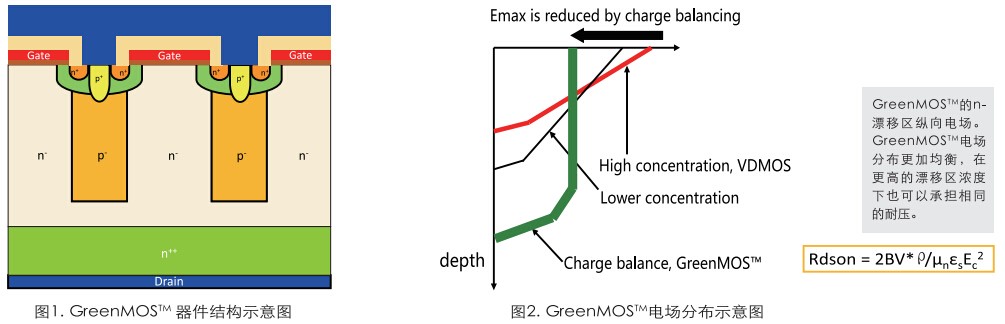
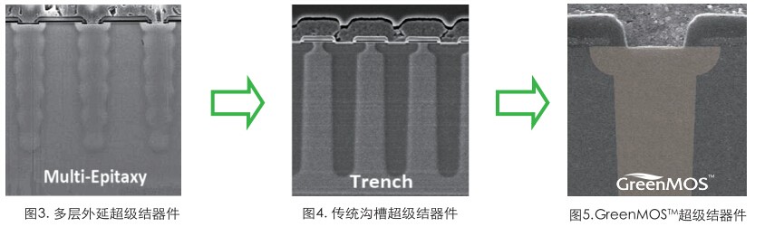
Dongwei The semiconductor GreenMOSTM device uses the technical principle of super junction (图 1). Based on its charge balancing technology, the substrate doping concentration can be greatly improved, and the characteristic on-resistance of the super junction device is greatly reduced. . The GreenMOSTM device further optimizes the process parameters, and the internal electric field of the device is more balanced (图 2), and the performance is also better and more stable. The superjunction device includes two fabrication processes: multiple epitaxy (图 3) and deep trench epitaxy (图 4). The former is costly, while the latter is prone to switching oscillations and causes electromagnetic compatibility (EMC) problems due to insufficient switching softness. GreenMOSTM has a patented process and device structure design that optimizes traditional technology (Figure 5), improves device switching softness and improves epitaxial defects, and solves the traditional super junction device EMC And reliability issues. Its high efficiency switching performance is close to that of expensive GaN devices, and the proven silicon processing technology makes GreenMOSTM devices extremely reliable.
|
| |
| Product Performance |
|
|
|
|
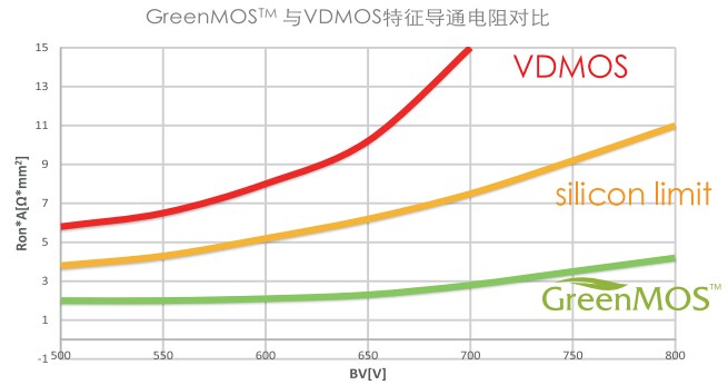
Figure 6. Comparison of GreenMOSTM and VDMOS characteristic on-resistance Ron(sP). The Ron(sP) of GreenMOSTM is lower than the silicon limit curve and much smaller than the conventional VDMOS. |
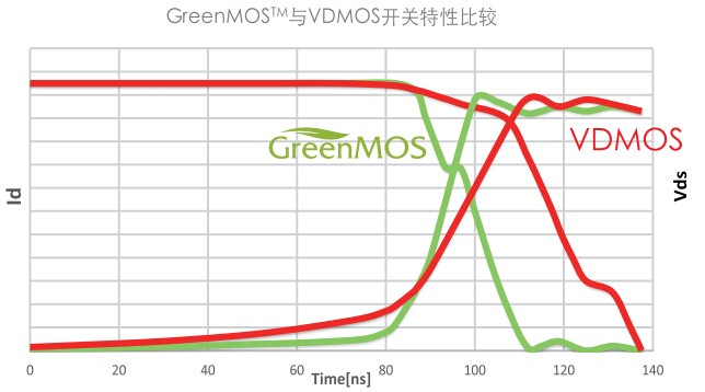
Figure 7. Comparison of GreenMOSTM and VDMOS switch characteristics. GreenMOSTM features high-speed switching and high-softness switching curves to reduce switching losses. |
| |
 |
 |
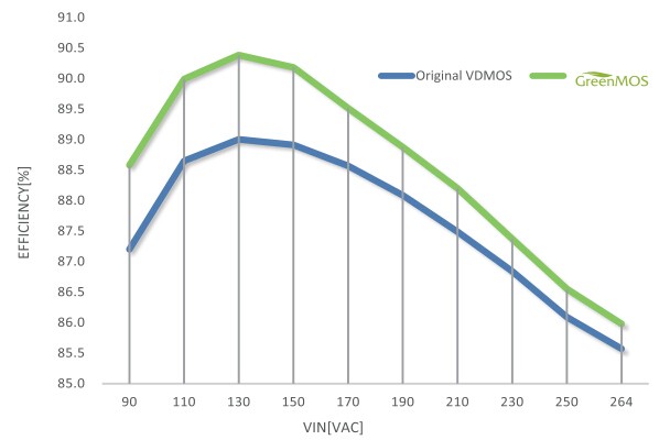
| Figure 8. GreenMOSTM is applied to the 24W LED Driver corresponding to the same specification VDMOS efficiency curve, the internal resistance is the same as 2.3ohm device, in the application of GreenMOSTM and increase the gate drive resistance, the efficiency is still greater than the VDMOS of the same specification. |
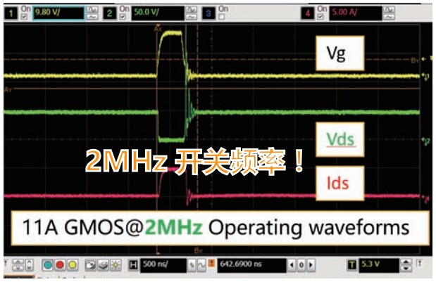
Figure 9. Due to the minimal Cgd of the GreenMOSTM device, its switching performance is close to that of the third-generation semiconductor GaN device, which can be used in 2-3MHz high voltage modules. And there is no obvious loss of efficiency. The system operating frequency is much higher than the traditional planar MOS and ordinary super junction devices. The high-frequency power system can take full advantage of the ultra-low FOM value of the GreenMOSTM device, greatly reducing the size of the system and improving system efficiency. |
| |
|
|
|
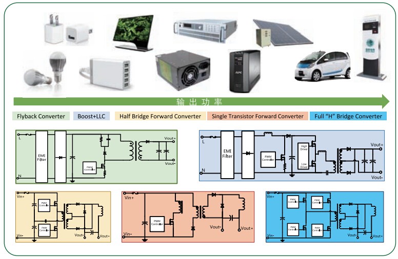
| Figure 10. GreenMOSTM and SFGMOSTM series products are widely used in various high-efficiency power systems. Its ultra-low on-resistance and switching loss greatly improve the conversion efficiency of the system, reduce the heat generation, and make the system design more flexible and cost-effective. |
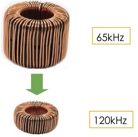
Figure 11. Lower cost gate driver circuit design; faster switching speed, especially in some highly integrated, modular product applications Higher frequency, effectively reducing volume and saving more cost; ultra-low on-resistance, improving system reliability and reducing heat sink material volume. |
CONQUER ELECTRONIC brand agent - Suzhou Oriental Semiconductor Co., Ltd. official website Get the latest information!
|
|
|
|


 Sale.
Sale.